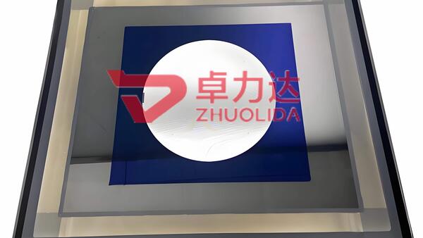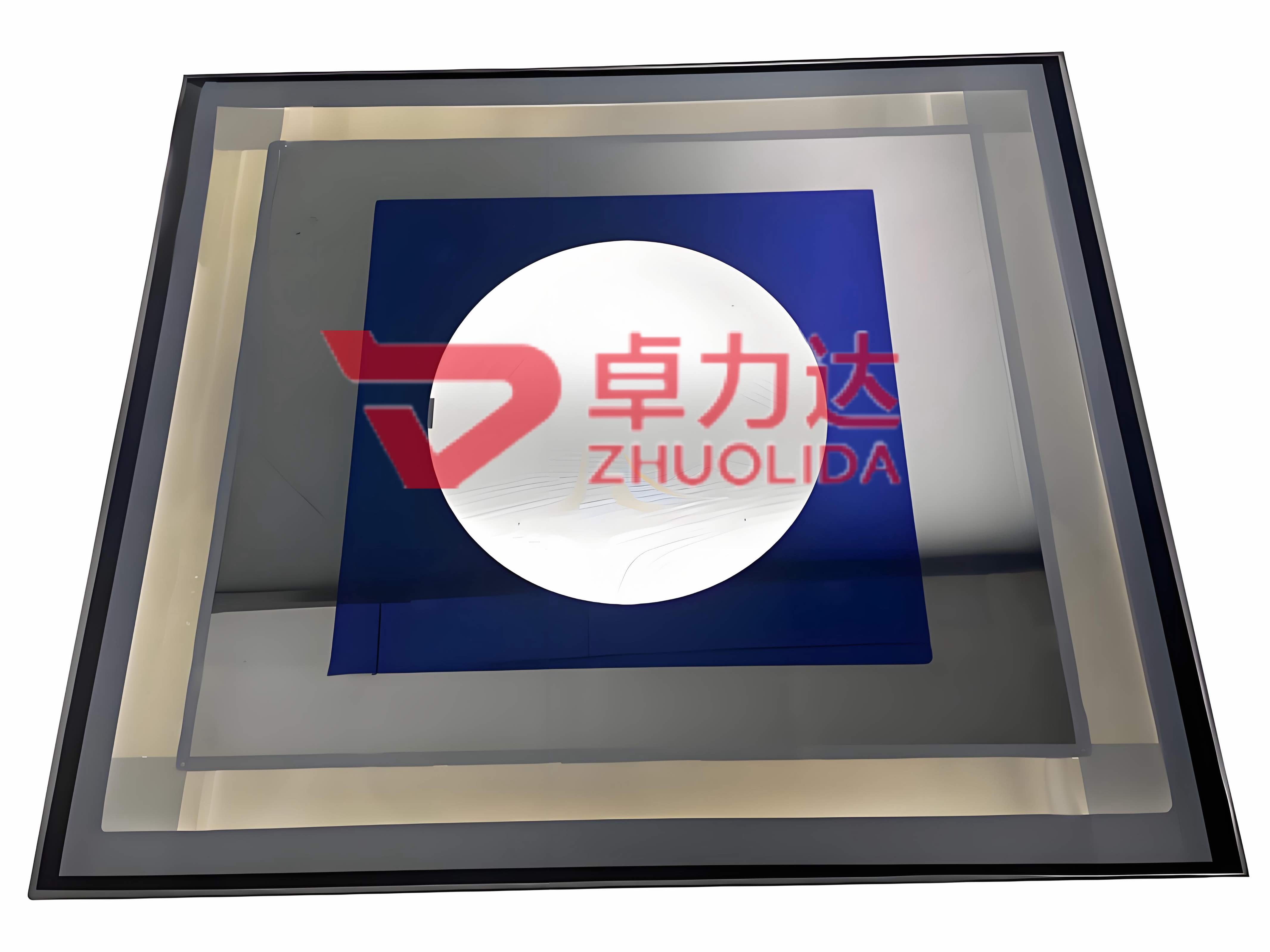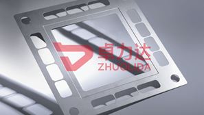
Our electroformed wafer template is precision-fabricated via electroforming technology. It delivers ultra-smooth surface, high dimensional accuracy and excellent repeatability for nanoimprint lithography and microfabrication. The rigid metal template supports high-volume wafer patterning, ensuring stable pattern transfer and long service life for semiconductor and MEMS manufacturing.
Electroformed Wafer Template: High Precision Electroformed Wafer Bumping Template for Semiconductor Packaging
In the fast-developing field of advanced semiconductor manufacturing and wafer-level packaging, high-precision micro-pattern processing tools are core to improving product yield and device stability, among which the Electroformed Wafer Template has become an indispensable key component for high-end wafer bumping and micro-pattern transfer. Also widely known as the Electroformed Wafer Bumping Template, this professional precision tool is manufactured through strict electroforming processes, completely different from traditional laser-cut and chemically etched wafer templates, and is widely applied in wafer-level packaging, flip chip bonding, 2.5D/3D IC stacking, HBM high-bandwidth memory packaging and MEMS microfabrication scenarios. With the continuous miniaturization of semiconductor chip structures and the gradual improvement of I/O density and packaging precision requirements, traditional processing templates can no longer meet the demands of ultra-fine pitch aperture processing, smooth sidewall molding and high-consistency solder paste release, making high-quality Electroformed Wafer Template the preferred choice for global semiconductor packaging enterprises and precision electronic manufacturing factories.
Nantong Zhuolida is a professional and reliable manufacturer focusing on Wafer Template, Electroformed Wafer Template and Electroformed Wafer Bumping Template, with years of rich experience in precision electroforming production and semiconductor supporting services. We independently develop and produce high-purity nickel electroformed wafer templates, covering mainstream wafer sizes such as 4-inch, 6-inch, 8-inch and 12-inch, and support full-customized aperture size, shape, template thickness and overall pattern design according to customers’ actual production needs. All our Electroformed Wafer Template products adopt additive electroforming molding technology, which grows metal materials layer by layer on the precision mold core, effectively avoiding the defects of burrs, uneven sidewalls and dimensional deviation easily caused by traditional subtractive processing technologies. This unique processing principle enables our wafer bumping templates to achieve micron-level ultra-high positioning accuracy and uniform aperture distribution, providing stable and reliable technical support for high-precision solder ball planting and solder paste printing of wafers.
The excellent performance of Electroformed Wafer Template is fully reflected in the actual semiconductor packaging production process. Different from laser stencils with thermal deformation and rough edge burrs and etched templates with inconsistent aperture wall thickness, our electroformed wafer bumping templates have smooth and regular trapezoidal sidewalls, which can realize clean solder paste and solder ball release during the printing and planting process, effectively reducing production defects such as solder bridging, missing bumps and offset bumps. While improving the qualified rate of wafer packaging products, it also greatly optimizes the consistency of solder bump height and shape on the wafer surface, ensuring the stable electrical performance and structural reliability of finished chips. In addition, the high-purity nickel material selected for our Electroformed Wafer Template has excellent mechanical stability, low thermal expansion coefficient and strong pressure resistance, which can maintain long-term dimensional stability under frequent squeegee extrusion and repeated processing cycles, with a far longer service life than traditional templates, effectively reducing the overall production cost and tool replacement frequency for customers.
Our customized Wafer Template and Electroformed Wafer Bumping Template have covered a full range of high-precision manufacturing scenarios in the semiconductor industry, including fan-in and fan-out wafer-level packaging for consumer electronic chips, RF chips and sensor chips, fine-pitch micro-bump packaging for high-performance CPU, GPU and AI accelerator chips, ultra-high density interconnection processing for 2.5D and 3D stacked chips and HBM memory chips, as well as high-stability packaging production for automotive-grade IGBT power semiconductors. At the same time, our products also adapt to MEMS micro-sensor processing, optical wafer patterning and microfluidic chip manufacturing, meeting the diversified precision processing needs of different industries and different process accuracies.
As a professional supplier rooted in precision electroforming technology, Nantong Zhuolida has a standardized clean production workshop and complete precision testing equipment, and every finished Electroformed Wafer Template will undergo multi-dimensional strict inspection including dimensional accuracy, aperture uniformity, surface flatness and sidewall smoothness before delivery to ensure that each product meets international semiconductor industry standards. We provide one-stop customized services from DFM scheme optimization, prototype trial production, sample testing to mass production, and our professional technical team can adjust the template structure and process parameters according to customers’ production equipment and process characteristics, perfectly matching customers’ high-precision wafer bumping production lines. In the era of increasingly stringent advanced semiconductor packaging precision standards, high-quality Electroformed Wafer Template has become a key factor to help enterprises improve production efficiency and market competitiveness. Nantong Zhuolida always adheres to high-precision, high-stability and high-customization product advantages, and provides cost-effective Wafer Template and Electroformed Wafer Bumping Template products and professional supporting services for global semiconductor manufacturing and packaging customers, helping customers complete high-yield and high-quality wafer micro-pattern processing and advanced packaging production.
Copper corrosion refers to the phenomenon of chemical or electrochemical reaction of copper and its alloys in specific environment (such as humid, sulfur-containing or salt-containing air), leading to the formation of copper corrosion on the surface (such as basic copper carbonate, copper sulfide, etc.).
Our electroformed stencil is a high-precision nickel SMT printing template made by electroforming. With ultra-smooth trapezoidal aperture walls, it delivers excellent solder paste release for ultra-fine pitch PCB assembly. Custom sizes, framed or frameless options are available. This electroformed stencil ensures consistent printing results, minimizes bridging and improves yield for micro BGA, flip chip and wafer bumping projects.
Microporous plate etching products cover a wide range of fields, including communications, acoustics, optics, medical, security, machinery, aviation, land transport tools, home appliances and so on.
Corrosion processing is a popular word for etching. The commonly referred to etching is also called photochemical etching. It refers to the removal of the protective film of the etching area through exposure to plate making and development.