
Product
FRIENDLY/link Nantong zhuolida Ali SAMSAN Corrosion machining Nantong zhuolida HJD Shenzhen zhuolida Esprit print
HOTLINE
189-3869-3452 0513-8160 1666

189-3869-3452 0513-8160 1666

As electronic devices keep shrinking in size, ultra-fine pitch PCB assembly and advanced semiconductor packaging have become mainstream demands across the electronics industry. Conventional laser-cut stencils often struggle with tiny apertures, rough sidewalls, solder bridging and inconsistent paste transfer in high-density circuits. This is where the electroformed stencil, also known as electroformed printing template, stands out as the premium solution for precision solder paste printing. Manufactured by Zhuolida, our electroformed stencil delivers unmatched dimensional accuracy, excellent solder paste release and stable printing performance for SMT assembly, micro BGA, flip chip and wafer bumping applications.
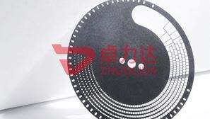
An electroformed stencil is a nickel-based SMT printing template produced by an additive electroforming process. Unlike laser cutting that removes material, electroforming deposits nickel atoms layer by layer onto a precision patterned mandrel. Photoresist defines the aperture geometry on the mandrel before nickel electroplating takes place. After metal deposition, the nickel foil is separated from the substrate, forming integrated apertures with naturally trapezoidal, ultra-smooth sidewalls. No thermal stress is generated during manufacturing, so there is no distortion, burr or slag on aperture edges. This unique manufacturing method makes electroformed stencils the ideal packaging printing template for advanced chip packaging projects.
Our Zhuolida electroformed stencil adopts advanced LDI lithography and pulse electroforming technology. The aperture tolerance can reach ±0.8μm, supporting ultra-small micro-apertures down to 5μm. The trapezoidal aperture walls greatly reduce solder paste adhesion, achieving paste transfer efficiency higher than 95%. Less paste residue inside holes reduces frequent under-stencil wiping and minimizes common printing defects such as bridging, insufficient solder and missing deposits. For high-volume mass production, our nickel-cobalt alloy electroformed stencil reaches HV500+ hardness, offering a much longer service life compared to standard stainless steel laser stencils.
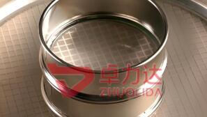
Flexible customization is one of the core strengths of our electroformed stencil. We supply both framed and frameless stencil foils. Variable thickness step stencils are available in one single foil, which meets mixed printing requirements for micro chips and large components on the same PCB. Thickness can be customized precisely in small increments to match your solder paste volume needs. Whether you need SMT printing stencils for consumer electronics, or packaging printing templates for semiconductor packaging, Zhuolida can tailor the electroformed stencil according to your Gerber files, pitch specifications and production environment.
Many manufacturing engineers wonder when to choose electroformed stencil instead of laser-cut stencil. Laser-cut stencils work well for standard SMT projects with pitch above 0.4mm. However, when you handle ultra-fine pitch components under 0.3mm, micro BGA, flip chip and wafer bumping, electroformed printing template is strongly recommended. Laser cutting creates slightly rough aperture walls, which easily traps solder paste and causes unstable printing results. Electroformed stencil solves these pain points with smooth trapezoidal walls and micron-level accuracy, directly improving assembly yield and lowering rework cost.
At Zhuolida, we maintain full in-house control over the entire electroformed stencil workflow, from photolithography, electroforming, surface treatment to AI visual inspection. Every electroformed stencil undergoes strict dimensional inspection before delivery to guarantee consistency batch after batch. Our factory is located in Nantong, China, serving global electronics manufacturers, EMS factories and semiconductor packaging customers. We provide technical consultation for stencil design optimization, helping customers select proper aperture ratios and foil thickness to fit different solder paste types and printing machines.
When selecting an electroformed stencil supplier, precision control, material quality and technical support matter more than price alone. A poorly manufactured electroformed stencil will still bring printing troubles and hurt your production yield. Zhuolida focuses on high-end electroformed printing template manufacturing. We support small-batch prototype stencils and mass production orders, with reliable lead time for overseas clients.
If your project involves ultra-fine pitch SMT assembly or advanced semiconductor packaging, our electroformed stencil is your reliable printing template partner. Contact Zhuolida today to share your Gerber data and printing requirements, and get a custom electroformed stencil solution for your next electronics manufacturing project.



 189-3869-3452 0513-8160 1666
 E-MAIL:yw5@zldsmt.com
 QQ:$qq
 No. 268, Jinchuan Road, Nantong high tech Industrial Development Zone, Tongzhou District, Nantong City, Jiangsu Province
All Rights Reserved © 2019-2030Nantong Zhuolida metal Technology Co., Ltd.
ICP:【苏ICP备17060045号-3】


 TEL
TEL Products
 News
News About us