HOTLINE

189-3869-3452 0513-8160 1666
  • Electroformed Test Probe Sheet
1/1
Electroformed Test Probe Sheet
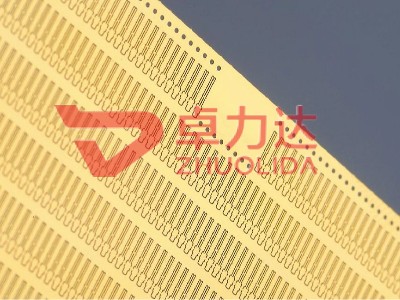
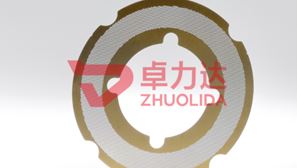
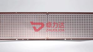
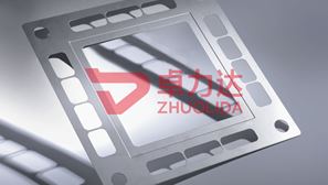
Fabricated by photolithography‑electroforming with nickel‑cobalt alloy. Stress‑free micro‑spring structure delivers stable low‑resistance contact. Supports custom pitch and gold‑plated surface, widely used for semiconductor wafer and IC high‑density testing.

189-3869-3452 0513-8160 1666

PRODUCT DETAILS

Electroformed Test Probe: High-Precision Micro Probes for Semiconductor Wafer Testing
Electroformed Test Probe is a high-end micro precision contact component manufactured via integrated photolithography and electroforming technology. As a core alternative to traditional pogo pins and machined probes, it has become an essential part of modern semiconductor wafer testing, IC inspection, MEMS device detection and high-density electronic measurement systems. Featuring ultra-small pitch, zero internal stress, stable electrical conductivity and long service life, the electroformed test probe perfectly meets the miniaturization and high-precision testing demands of next-generation electronic components.

Different from conventional probe processing methods such as mechanical drilling, laser cutting and stamping, electroformed test probes are produced through additive metal deposition rather than material removal. The entire manufacturing process relies on precision mold preparation, photoresist patterning, pulse electroforming, alloy deposition and precision post-treatment. This advanced EFC (Electro Formed Components) technology effectively eliminates common defects including burrs, thermal deformation, residual stress and uneven surface roughness that plague traditional probes. The finished probes deliver ultra-smooth surfaces with roughness below 0.1μm, ensuring damage-free contact with tiny chip pins and wafer circuits.

The core technical advantages of electroformed test probes are reflected in dimensional accuracy and structural stability. The product supports micro-sized customized structures, including ultra-thin probe sheets, micro-spring contact structures, dense probe arrays and special-shaped contact terminals. It achieves a minimum testing pitch of 0.175mm, which is far superior to traditional cylindrical probes in high-density array arrangement. Made of high-purity nickel or nickel-cobalt alloy with optional gold or rhodium plating on the contact surface, the probe maintains extremely low and stable contact resistance during long-term repeated testing, avoiding signal attenuation and test data deviation.

Structurally optimized for professional testing scenarios, electroformed test probes integrate flexible micro-spring structures. The one-piece electroformed molding design requires no assembly, effectively solving loose positioning, poor elasticity and easy fracture problems of assembled probes. After tens of thousands of compression and contact cycles, the probe can still maintain stable mechanical resilience and precise positioning accuracy, greatly reducing replacement frequency and equipment maintenance costs. The stress-free metal structure ensures no deformation or fatigue failure under long-term high-temperature and high-load working conditions, adapting to rigorous semiconductor factory testing environments.

                                            dd0833977c934ed2af53f0c2c527c419_30

Electroformed test probes have irreplaceable application value in multiple high-tech fields. In semiconductor wafer testing, high-density electroformed probe arrays support batch testing of tiny wafer electrodes, improving testing efficiency and accuracy for chip packaging and sorting. In IC component inspection, ultra-thin micro probes can access narrow and complex test positions that traditional probes cannot reach, realizing comprehensive detection of precision circuit boards and miniaturized electronic components. In addition, they are widely used in MEMS sensor testing, automotive electronic component detection, aerospace precision circuit inspection and laboratory high-precision electrical measurement.

Compared with traditional test probes, electroformed probes show obvious comprehensive performance advantages. Traditional pogo pins are limited by cylindrical structure, with large spacing occupation and poor adaptability to high-density miniature circuits. Machined probes are prone to burrs and surface scratches, which easily damage tiny test points and cause poor electrical contact. In contrast, electroformed test probes feature flexible customizable shapes, ultra-high flatness, consistent batch performance and excellent electrical conductivity, making them the preferred solution for high-precision and high-density testing scenarios.

Professional manufacturers optimize electroformed test probes through full-process precision control, from mold manufacturing and electroforming deposition to surface plating and full visual inspection. Strict dimensional tolerance control and surface treatment ensure each probe has consistent elasticity, contact performance and service life. Custom services for different thicknesses, pitches, shapes and plating requirements are available to meet personalized testing needs of various industries.

With the continuous miniaturization and high integration of semiconductor and electronic products, the industry puts forward higher requirements for the precision, stability and durability of test components. As a high-performance precision testing component, the electroformed test probe will continue to replace traditional probes in high-end testing fields. It provides reliable, high-efficiency and low-consumption contact testing solutions for global semiconductor, electronic manufacturing and precision detection industries, becoming a key basic component supporting the upgrading of modern precision testing technology.


PRODUCT CHARACTERISTICS

HOT PRODUCT
Micro hole machining

Micro hole machining

Product description product name: micro hole processing product introduction: as the name implies is in the need to process the workpiece with chemical etching process or other processes to process small holes.Applications: widely used in precision filtration equipment, chemical fiber spinnerets, jet engine nozzles, computer print heads, printed circuit boards, television baffles, astrology star orifice plates, aviation gyroscope instrument components, aircraft turbine blades and medical equipment in red blood cell filters...
Vacuum cleaner strainer

Vacuum cleaner strainer

Vacuum cleaner filter, as a filter element, is a key link in the filtering process of vacuum cleaner. The quality of vacuum cleaner filter determines the filtering effect of vacuum cleaner to a large extent.The vacuum cleaner filtaer with etching process has no burr and good flatness.
Copper corrosion

Copper corrosion

Copper corrosion refers to the phenomenon of chemical or electrochemical reaction of copper and its alloys in specific environment (such as humid, sulfur-containing or salt-containing air), leading to the formation of copper corrosion on the surface (such as basic copper carbonate, copper sulfide, etc.).
The corrosion process

The corrosion process

Corrosion processing is a popular word for etching. The commonly referred to etching is also called photochemical etching. It refers to the removal of the protective film of the etching area through exposure to plate making and development.