
Product
FRIENDLY/link Nantong zhuolida Ali SAMSAN Corrosion machining Nantong zhuolida HJD Shenzhen zhuolida Esprit print
HOTLINE
189-3869-3452 0513-8160 1666


189-3869-3452 0513-8160 1666

An electroformed aperture is a high‑performance metal optical component manufactured by photolithography and electroforming additive technology, widely used to shape, limit and block stray light in precision optical systems. Unlike aperture parts produced by laser cutting, chemical etching or mechanical drilling, electroformed apertures grow metal atom‑by‑atom on a pre‑patterned conductive mandrel, rather than removing material from bulk metal sheets. This additive manufacturing principle delivers micron‑level dimensional accuracy, sharp burr‑free aperture edges and stress‑free metal structures, solving typical defects including thermal deformation, micro‑slag, edge burrs and rough inner walls that frequently appear in subtractive‑manufactured aperture plates.
The core production workflow of electroformed aperturecovers substrate cleaning, photoresist coating, UV exposure, chemical development, nickel electrodeposition, demolding and post‑surface treatment. First, a flat conductive mandrel is thoroughly cleaned and degreased to eliminate surface contaminants. Light‑sensitive photoresist material is evenly coated on the mandrel surface. Next, UV‑LDI exposure transfers the designed aperture pattern onto photoresist layers. During developing processes, un‑exposed photoresist is dissolved away, leaving raised photoresist pillars which define the final hollow aperture geometry. After that, the patterned mandrel is submerged in nickel‑based electrolytic bath. Under stable direct‑current control, pure nickel or nickel‑cobalt alloy continuously deposits around photoresist pillars until target foil thickness is achieved. The finished aperture sheet is peeled off from the mandrel, followed by cleaning, stress‑relief heat treatment and optional surface blackening coating for low‑reflective performance.
Electroformed apertures own irreplaceable technical strengths for high‑end optical scenarios. Dimensional tolerance can reach ±0.5‑1 μm, aperture edge sharpness stays below 0.1 μm with nanometer‑scale inner‑wall roughness. No internal residual stress exists inside electroformed nickel sheets, so components keep stable flatness after long‑time operation and temperature cycling, avoiding shape distortion which would deteriorate beam quality. Custom geometries are highly flexible: single circular holes, long slits, square openings and large‑scale complex aperture arrays can be realized in one forming step. Thickness ranges from 0.01 mm up to 0.2 mm according to customer requirements. Black‑nickel or DLC surface coating is available to suppress stray‑light reflection down to low single‑digit percentage, critical for high‑signal‑to‑ratio optical detection equipment.
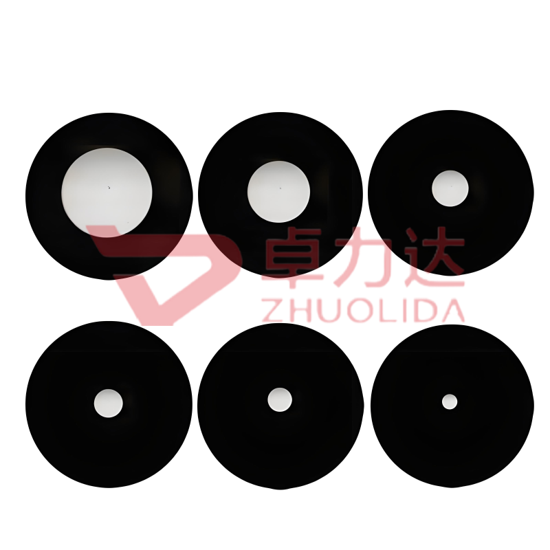
These unique properties make electroformed aperture adopted across multiple high‑tech industries. In laser systems, they constrain beam diameter, filter scattered light and improve laser spot uniformity. For semiconductor inspection instruments, ultra‑precise aperture arrays support micron‑scale optical detection on wafer surfaces. In medical imaging devices such as digital radiography and optical diagnostic equipment, electroformed apertures help enhance imaging resolution and reduce background noise. They also serve scientific instruments, aerospace optical payloads and high‑speed optical measuring apparatus, where consistent optical performance under demanding working conditions is mandatory.
Many design engineers struggle when selecting aperture components. Laser‑cut apertures feature fast lead‑time and competitive pricing, yet heat‑affected zones and micro‑burrs are hard to eliminate for sub‑20 μm tiny holes. Chemical‑etched apertures suffer from undercut effect, limiting minimum achievable aperture dimension and geometric accuracy. Mechanical drilling cannot produce dense array micro‑holes or narrow slits economically. In contrast, electroformed aperture becomes the preferred solution whenever sub‑millimeter or micron‑level apertures, sharp edge profile and high batch‑to‑batch consistency are non‑negotiable requirements. Nevertheless, electroforming requires custom mandrel tooling, which leads to higher tooling cost and moderately longer lead‑time compared with laser‑cut alternatives, making it more suitable for high‑precision prototyping and medium‑volume mass‑production rather than low‑accuracy, cost‑only‑oriented projects.
When sourcing electroformed aperture plates, buyers should verify key performance indicators: aperture dimensional tolerance, edge radius, flatness, surface roughness, material composition and anti‑reflective coating indexes. Reliable suppliers shall provide dimension inspection reports, material certificates and sample validation before mass manufacturing. Zhuolida delivers custom electroformed aperture solutions, covering design consultation, prototype validation and serial production, supporting diverse custom patterns and surface treatment options for global optical and industrial customers.
As optical hardware keeps advancing toward higher resolution, miniaturization and stronger anti‑interference capacity, market demand for high‑quality electroformed aperture will keep expanding. Understanding electroforming technical characteristics, advantages and limitations assists system designers to make proper component selection and optimize overall optical‑system performance.




 189-3869-3452 0513-8160 1666
 E-MAIL:yw5@zldsmt.com
 QQ:$qq
 No. 268, Jinchuan Road, Nantong high tech Industrial Development Zone, Tongzhou District, Nantong City, Jiangsu Province
All Rights Reserved © 2019-2030Nantong Zhuolida metal Technology Co., Ltd.
ICP:【苏ICP备17060045号-3】


 TEL
TEL Products
 News
News About us