
Product
FRIENDLY/link Nantong zhuolida Ali SAMSAN Corrosion machining Nantong zhuolida HJD Shenzhen zhuolida Esprit print
HOTLINE
189-3869-3452 0513-8160 1666

189-3869-3452 0513-8160 1666

BGA Package Printing Stencil | High Precision BGA Electroformed Stencil from Nantong Zhuolida
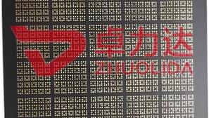
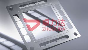
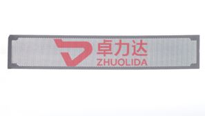
The BGA package printing stencil is a critical precision tool for SMT solder paste printing and semiconductor packaging processes. Also known as BGA electroformed stencil, BGA printing electroformed stencil or simply BGA electroformed stencil, it directly controls solder paste deposition volume, shape and uniformity on ball grid array pads. For electronics manufacturers, packaging houses and PCBA factories, choosing a reliable BGA package printing stencil is one of the most effective ways to reduce production defects including solder bridging, voiding, insufficient solder and poor ball formation.
As electronic devices keep shrinking, BGA, micro-BGA and FC-BGA packages adopt ultra-fine pitch layouts. Traditional standard stencils struggle to deliver consistent paste release for dense BGA pad arrays. Poor aperture wall quality often traps solder paste during printing, leading to unstable solder joints and low first-pass yield. This is where high-end BGA electroformed stencils stand out. Nantong Zhuolida specializes in manufacturing custom BGA package printing stencils and BGA electroformed stencils for semiconductor packaging, automotive electronics, medical devices, communication modules and industrial PCBA applications.
There are two mainstream types of BGA printing templates widely used in SMT and packaging production: laser-cut stainless steel BGA package printing stencils and nickel BGA electroformed stencils. Laser-cut BGA stencils offer balanced precision and cost performance for standard pitch BGA components. They are widely adopted for prototype runs and mass PCBA assembly. However, for ultra-fine pitch BGA packaging below 0.35 mm, electroformed BGA stencils become the preferred option. Manufactured through nickel electro-deposition technology, BGA electroformed stencils feature perfectly smooth, vertical aperture walls with no burrs or undercuts. The ultra-smooth inner walls greatly improve solder paste release rate, minimizing paste residue inside tiny BGA circular apertures. Compared with laser alternatives, BGA electroformed stencils maintain stable printing results over far more printing cycles, making them ideal for high-volume semiconductor packaging lines.
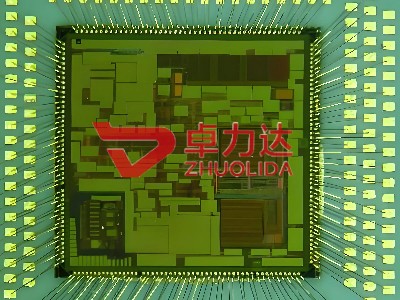
At Nantong Zhuolida, every BGA package printing stencil is custom fabricated according to customers’ Gerber files, pitch specifications, stencil thickness and aperture reduction requirements. Our engineering team carries out DFM checks before production to optimize BGA aperture design, preventing bridging and void issues at the source. We can manufacture BGA electroformed stencils with micron-level positional accuracy, suitable for FC-BGA, uBGA and high-density chip packaging. Our electroformed stencil surface roughness is controlled at Ra ≤0.1μm, ensuring excellent paste transfer consistency for densely arranged BGA ball pads. Apart from standard flat stencils, we also offer step stencil solutions when mixed components share one printing frame.
Many electronics engineers encounter recurring printing challenges when working with fine-pitch BGA packages. Common pain points include inconsistent solder paste height, frequent bridging between adjacent BGA pads, random voids after reflow, and fast stencil wear during continuous mass production. These problems are usually caused by poor aperture geometry, rough hole walls or improper stencil thickness selection. Our BGA package printing stencils and BGA electroformed stencils are engineered to solve these typical pain points. The smooth vertical nickel apertures of BGA electroformed stencils ensure nearly complete solder paste release every print cycle. Stable paste volume on each BGA pad guarantees uniform solder ball formation after reflow, significantly raising assembly yield and cutting rework costs for packaging factories.
Nantong Zhuolida is a professional manufacturer based in Nantong, China, focusing on precision metal stencils for semiconductor packaging and SMT industry. We combine years of electroforming and precision machining experience to supply BGA package printing stencils and BGA electroformed stencils for global customers. From small batch prototype stencils to large volume mass production stencils, we maintain strict quality inspection for each finished stencil. Each BGA stencil will go through optical dimension inspection before shipment to verify aperture size, position tolerance and surface quality. Fast Gerber evaluation, flexible customization and stable lead time make us a trusted supplier for overseas electronics packaging and SMT assembly companies.
When selecting a BGA package printing stencil or BGA electroformed stencil, buyers should evaluate multiple factors: BGA pitch, required solder paste volume, production batch size, printing machine compatibility and reliability standards. For automotive electronics and aerospace semiconductor packaging where high reliability is mandatory, BGA electroformed stencils are strongly recommended due to their superior repeatability and long service life. For regular BGA packages with larger pitch, laser-cut BGA printing stencils provide a cost-effective alternative. Our technical team at Zhuolida can analyze your PCB or package design and recommend the most suitable stencil type, thickness and aperture modification solution according to your actual production requirements.
If you are sourcing high-quality BGA package printing stencils, BGA package electroformed stencils, BGA printing electroformed stencils or BGA electroformed stencils for your SMT or semiconductor packaging line, contact Nantong Zhuolida today. Send us your Gerber files and BGA specifications, and our sales and engineering team will provide professional technical support and competitive quotation.


 189-3869-3452 0513-8160 1666
 E-MAIL:yw5@zldsmt.com
 QQ:$qq
 No. 268, Jinchuan Road, Nantong high tech Industrial Development Zone, Tongzhou District, Nantong City, Jiangsu Province
All Rights Reserved © 2019-2030Nantong Zhuolida metal Technology Co., Ltd.
ICP:【苏ICP备17060045号-3】


 TEL
TEL Products
 News
News About us