
Product
FRIENDLY/link Nantong zhuolida Ali SAMSAN Corrosion machining Nantong zhuolida HJD Shenzhen zhuolida Esprit print
HOTLINE
189-3869-3452 0513-8160 1666

189-3869-3452 0513-8160 1666

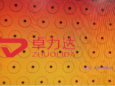
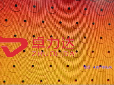
An electroformed nickel stencil is a high-precision SMT printing tool manufactured through professional electroforming technology, widely adopted in advanced PCB assembly and microelectronic manufacturing. Different from traditional laser-cut and chemically etched stencils, the nickel electroformed stencil is formed by layer-by-layer nickel ion deposition, featuring ultra-smooth aperture walls, micron-level dimensional accuracy and stable structural performance. For high-end electronic production scenarios requiring ultra-fine pitch printing, the custom electroformed nickel stencil has become the optimal solution to solve common printing defects such as solder paste bridging, insufficient tin deposition and uneven printing, ensuring high yield and consistent mass production results.
With the continuous miniaturization of electronic components, traditional stencils can no longer meet the processing requirements of 0.3mm ultra-fine pitch, micro BGA, QFN and tiny chip packaging. Laser-cut stencils often produce rough aperture walls and burrs, while etched stencils suffer from uneven aperture size and poor repeatability. In contrast, the electroformed nickel stencil perfectly overcomes these drawbacks. Made of 99.9% high-purity nickel material, it features uniform metal grain structure, low friction coefficient and excellent solder paste release performance, greatly improving the transfer efficiency of ultra-fine solder paste. It has become a standard precision accessory in high-volume, high-precision SMT production lines.
The core advantage of the nickel electroformed stencil stems from its unique non-destructive electroforming manufacturing process, which is completely different from the material removal processing of traditional stencils. The whole production process adopts photolithography and electrodeposition technology without high-temperature cutting and chemical corrosion, avoiding thermal deformation and structural stress. Manufacturers first make precision photoresist patterns on the mold core according to customer PCB design drawings, then deposit pure nickel atoms uniformly through electroplating, and finally peel off and finish the stencil foil.
This bottom-up growth molding technology enables each aperture of the custom electroformed nickel stencil to achieve trapezoidal smooth wall structure with no burrs, no pits and no uneven edges. The dimensional tolerance can be controlled within the micron level, and the consistency of each batch of products is extremely high. In addition, the electroforming process can flexibly customize stencil thickness, aperture shape, hole wall gradient and frame structure according to different printing processes, realizing personalized customization for diverse industrial production needs.
Compared with stainless steel laser stencils and chemical etched stencils, the electroformed nickel stencil has irreplaceable performance advantages in precision printing scenarios. Firstly, it delivers excellent solder paste release. The ultra-smooth aperture wall greatly reduces the friction between solder paste and the hole wall, effectively avoiding paste residue and blockage. The solder paste transfer efficiency can reach more than 90%, which significantly reduces defective products caused by insufficient tin and uneven printing.
Secondly, it supports ultra-fine pitch high-precision printing. Traditional stencils are prone to bridging and tin connection when printing tiny pads, while the nickel electroformed stencil with precise aperture design can perfectly adapt to ultra-fine spacing components such as 0.2mm and 0.3mm pitch, meeting the manufacturing standards of high-precision consumer electronics, automotive electronics and communication equipment. Meanwhile, high-purity nickel material has higher hardness and tensile strength, with strong deformation resistance, effectively extending the service life and reducing the frequency of stencil replacement in mass production.
In addition, the custom electroformed nickel stencil has outstanding batch stability. The electroforming process does not produce thermal stress and chemical corrosion traces, ensuring consistent aperture size and flatness of each stencil. Whether it is small-batch prototype proofing or large-batch continuous production, it can maintain stable printing accuracy, effectively reduce production error rates and improve overall production efficiency.
The high-precision and high-stability characteristics of the electroformed nickel stencil make it widely used in high-end electronic manufacturing fields. In the consumer electronics industry, it is used for SMT printing of mobile phone chips, tablet components and wearable devices, adapting to the ultra-thin and miniaturized production requirements of precision electronic products. In automotive electronics manufacturing, it supports the production of vehicle-mounted control modules, sensor components and new energy electronic parts, ensuring high reliability of electronic components in complex working environments.
In the fields of medical electronics, aerospace precision equipment and 5G communication devices, the nickel electroformedstencil undertakes ultra-fine circuit printing work. Its high precision and stable performance effectively avoid circuit short circuit and poor welding caused by printing errors, ensuring the safety and stability of high-end equipment operation. At the same time, customized models are also widely used in semiconductor packaging, micro-module processing and precision instrument circuit production, covering almost all high-precision SMT printing scenarios.
Professional custom electroformed nickelstencil supports full-dimensional personalized customization to match different production processes and equipment parameters. Customers can customize stencil thickness ranging from ultra-thin 0.08mm to conventional 0.15mm according to solder paste type and component density. The aperture structure can be optimized with trapezoidal, rectangular and special-shaped holes according to PCB pad distribution, effectively improving printing adaptability.
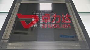
In terms of structural configuration, it supports framed and frameless dual styles, compatible with various mainstream SMT printing equipment. It can also customize anti-stress edges, reinforcement zones and special transition holes to solve printing problems such as easy deformation of thin stencils and uneven local tin volume. All customized products strictly follow international electronic manufacturing standards, with precise size control and stable quality, meeting the quality requirements of high-end export electronic products.
In modern electronic manufacturing, printing precision directly determines the product yield and service life. Ordinary low-precision stencils will lead to a large number of defective products, increasing production costs and after-sales pressure. The high-quality electroformed nickel stencil effectively solves the pain points of traditional printing processes. With ultra-smooth hole walls, micron-level precision, high wear resistance and excellent paste release performance, it greatly improves the yield of precision electronic products.
Professional manufacturers adopt dust-free workshop production and strict multi-process quality inspection for each batch of nickel electroformedstencil , including flatness detection, aperture size calibration, wear resistance test and printing effect verification. Every customized product can maintain high consistency and stability, helping electronic manufacturing enterprises optimize production processes, reduce defective rates and enhance market competitiveness.
As the core precision accessory of advanced SMT printing technology, the electroformed nickelstencil has become an indispensable tool in high-end electronic manufacturing by virtue of its ultra-high precision, excellent printing performance and durable structural stability. Different from traditional stencil products, the custom electroformed nickel stencil can flexibly adapt to various ultra-fine pitch and high-precision printing scenarios, effectively improving solder paste transfer efficiency and product yield. With the continuous upgrading of electronic manufacturing technology, electroformed nickel stencils will be more widely used in precision electronics, automotive, medical and communication fields, providing stable and reliable technical support for high-quality electronic batch production.



 189-3869-3452 0513-8160 1666
 E-MAIL:yw5@zldsmt.com
 QQ:$qq
 No. 268, Jinchuan Road, Nantong high tech Industrial Development Zone, Tongzhou District, Nantong City, Jiangsu Province
All Rights Reserved © 2019-2030Nantong Zhuolida metal Technology Co., Ltd.
ICP:【苏ICP备17060045号-3】


 TEL
TEL Products
 News
News About us