
Product
FRIENDLY/link Nantong zhuolida Ali SAMSAN Corrosion machining Nantong zhuolida HJD Shenzhen zhuolida Esprit print
HOTLINE
189-3869-3452 0513-8160 1666

189-3869-3452 0513-8160 1666

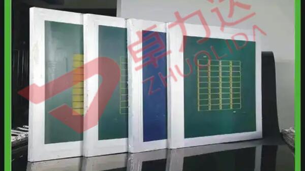
A PV screen printing stencil is a professional precision printing tool specially developed for photovoltaic solar cell metallization processes. As a core consumable in solar cell production, it undertakes the key task of printing silver paste, aluminum paste and conductive materials on silicon wafer surfaces to form fine grid lines and conductive circuits. Traditional screen printing tools struggle to meet the upgrading demands of high-efficiency solar cells, while a high-precision PV screen printing stencil features uniform aperture distribution, smooth line printing and stable paste release performance. It effectively reduces shading loss, lowers silver consumption, and improves cell conversion efficiency, becoming an essential component for mass production of TOPCon, PERC and high-end photovoltaic cells.
With the continuous iteration of photovoltaic technology, solar cells are developing toward thin wafers, fine grid lines and high conversion efficiency. Conventional low-precision printing stencils often cause problems such as uneven paste coating, broken grid lines and excessive material waste in the production process. The optimized photovoltaic screen printing stencil perfectly solves these industry pain points. Through precise structural design and high-standard manufacturing technology, it achieves ultra-fine line printing, stable thickness control and excellent repeatability. For photovoltaic manufacturers pursuing high yield, low cost and high efficiency, customized PV screen printing has become a key factor in improving core production competitiveness.
The working principle of the PV screen printing stencil relies on precise pattern penetration and uniform paste transfer. The stencil is designed with customized hollow grid patterns according to solar cell circuit specifications. During the printing process, conductive paste evenly passes through the stencil apertures and adheres to the fixed position of the silicon wafer surface under the pressure of the printing scraper, forming orderly and smooth conductive grid lines. The accuracy of the stencil’s aperture size, wall smoothness and overall flatness directly determines the fineness and uniformity of the printed grid lines.
Different from ordinary printing stencils, the photovoltaic screen printing stencil adopts professional photolithography and precision etching or electroforming technology. It ensures consistent aperture spacing and smooth hole walls without burrs or deformation. This precise structure enables the conductive paste to be released completely, avoiding paste residue, grid line bulging or edge burrs. It maintains high consistency of each printed cell circuit, laying a solid foundation for stable photoelectric conversion performance of photovoltaic modules.
The upgraded PV screen printing stencil has irreplaceable performance advantages compared with traditional screen printing tools in photovoltaic production. Firstly, it supports ultra-fine grid line printing. It can realize narrow and uniform fine line printing, effectively reducing the shading area of the solar cell surface, lowering light loss, and significantly improving the photoelectric conversion efficiency of cells. This feature is particularly critical for high-efficiency battery technologies such as TOPCon and HJT.
Secondly, the photovoltaic screen printing stencil greatly reduces silver paste consumption. Its smooth aperture wall ensures full paste release without residual accumulation, which cuts down the waste of expensive silver conductive paste and effectively reduces the production cost of photovoltaic cells. In large-scale mass production, this cost-saving advantage can bring huge economic benefits to manufacturers and optimize the overall profit margin of photovoltaic modules.
In addition, the PV printing stencil has excellent durability and stable batch consistency. Made of high-strength and wear-resistant materials, it can withstand long-term high-frequency printing operations without deformation, aperture expansion or pattern distortion. It features long service life and low replacement frequency, which improves the continuous production capacity of the production line and reduces equipment downtime and maintenance costs. The stable printing effect ensures uniform product quality of each batch of solar cells and reduces defective rates.
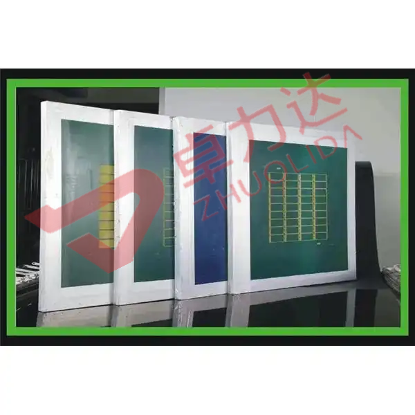
High-performance PV screen printing stencil adopts industry-specific high-quality materials and optimized structural design to adapt to harsh continuous production environments. Most high-end stencils use high-tension metal or high-performance PI composite materials, which have outstanding tensile resistance, wear resistance and anti-deformation ability. The materials can resist repeated scraping and friction during high-frequency printing, maintaining long-term structural stability.
In terms of structure, the photovoltaic screen printing stencil adopts precise grid layout and trapezoidal aperture optimization design. The gradient hole wall structure is conducive to rapid and complete paste release, preventing paste clogging and printing defects. The overall flatness of the stencil is strictly controlled to ensure close fitting with silicon wafers during printing, avoiding virtual printing, missing printing and uneven paste thickness. Meanwhile, customized tension reinforcement design effectively prevents stencil deformation during operation, further improving printing accuracy.
The PV screen printing stencil covers the full-process printing links of mainstream solar cell production. It is widely used in front and back electrode printing of PERC solar cells, fine grid printing of TOPCon high-efficiency cells, and conductive pattern processing of HJT heterojunction cells. It is suitable for M6, M10, G12 and other mainstream sizes of silicon wafers, meeting the production needs of different specifications of photovoltaic cells.
In industrial mass production, the PV printing stencil is mainly used for silver paste front grid printing, aluminum paste back field printing and conductive electrode secondary printing. It can stably complete high-precision printing operations in high-speed automated production lines, ensuring the consistency of cell electrode patterns and electrical performance. In addition, customized stencils can also be used for photovoltaic cell sample proofing, new process testing and special specification cell production, supporting technological innovation and product iteration of photovoltaic enterprises.
Facing the differentiated production needs of different photovoltaic processes and cell specifications, professional PV screen printing stencil supports full-dimensional personalized customization. Customers can customize grid line width, aperture spacing, pattern layout and stencil size according to battery design parameters and production equipment models. For high-efficiency battery production with ultra-fine grid line requirements, ultra-narrow aperture customized stencils can be provided to maximize cell conversion efficiency.
At the same time, the photovoltaic screen printing stencil supports customized tension adjustment, surface anti-sticking treatment and wear-resistant reinforcement processing. The optimized surface treatment can reduce paste adhesion, improve printing fluency and extend service life. Whether it is small-batch customized stencils for laboratory research and development or large-batch standardized stencils for industrial mass production, it can maintain high-precision and high-stability printing effects, perfectly matching diverse photovoltaic production scenarios.
As a core precision consumable in the photovoltaic cell manufacturing industry, the PV screen printing stencil plays a decisive role in improving cell conversion efficiency, reducing production costs and stabilizing product quality. The high-precision, durable and customizable photovoltaic screen printing stencil and professional PV printing stencil solutions perfectly adapt to the iterative upgrading of modern high-efficiency photovoltaic cell technology. Choosing high-quality PV screen printing stencils can effectively optimize the printing process of photovoltaic production lines, reduce resource waste and defective rates, and help photovoltaic enterprises gain greater competitive advantages in the high-efficiency solar energy market.


 189-3869-3452 0513-8160 1666
 E-MAIL:yw5@zldsmt.com
 QQ:$qq
 No. 268, Jinchuan Road, Nantong high tech Industrial Development Zone, Tongzhou District, Nantong City, Jiangsu Province
All Rights Reserved © 2019-2030Nantong Zhuolida metal Technology Co., Ltd.
ICP:【苏ICP备17060045号-3】


 TEL
TEL Products
 News
News About us